

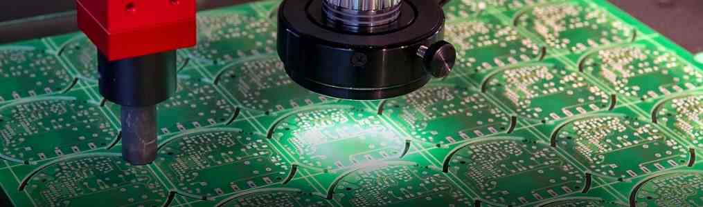
Before starting any development work it is critical to understand product and industry requirements and capabilities. If this is not fully understood, no development activities can start. PCB fabrication can be seen as a good example on the importance of understanding requirements and capabilities. If a good quality PCB canĄŊt be sourced within the scope of the assembly development project there is no reason to develop an assembly technology process since there is not anything to do the assembly development work on. The key is to ensure that several options for assembly can be achieved and this should be seen as a toolbox of technologies.
For the active components die stacking inside a package is one common way to increase the functionality per unit area on a PCBA, which is very popular for memory devices. However, there can be some drawbacks to creating a stacked die solution. First, this method is a customized solution. If any of the dies to be used changes, the die stack needs to be evaluated to see if changes are needed in the package. For example, a die shrink may occur and this could change the whole package structure. Secondly, if one or more of the dies inside the package fail, the whole unit will have to be scrapped, which would lead to increased cost; this is the well-known compounded yield issue. Lastly, trying to coordinate the many semiconductor suppliers to provide dies to a packaging house for die stacking can be a challenging task and overall responsibility for the complete package yield could in some cases be unclear.
In the PoP process one component is placed on top of another package during a single SMT process to fully utilize the three dimensional aspect of the product. The topside of the bottom component has pads similar to the pads on the PCB for attachment of the top package. Each package is a single unit that can be fully tested as a normal IC package is done today, so the yield would be comparable to the normal yield commonly seen today. Another advantage would be the ability to have second-source options that could be fairly easily inserted into the process.
The stacked package can be processed in a traditional SMT environment with a few upgrades that are readily available. Therefore, package stacking enables configurable assemblies and provides greater flexibility in the supply chain. It can be used for memory applications or for a processor with memory, with faster time to market and better management of package testing and compounded yield issues.
Tags: PCB manufacturer, PCB supplier, PCB assembly, PCB design, Multilayer PCB, HDI PCB, LED PCB, Automotive PCB, High Frequency PCB. Industry Control PCB, PCBA, PCB Samples.