

Unlike printing paste, placing components and reflowing solder, ICT is considered a non-value added process. In fact, ICT increases the cycle time of the assembly process. If the ICT is a fail, but the circuit being tested is actually good (known as a false negative), even more time is wasted trying to determine whether or not a good assembly will function properly.
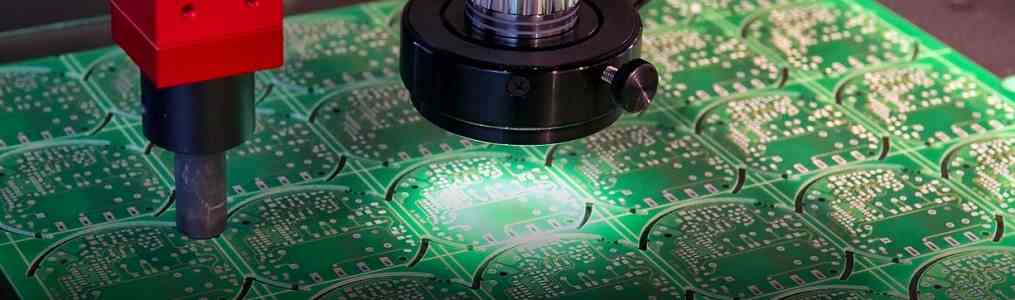
The two basic types of ICT are commonly referred to as clamshell and flying probe. The clamshell ICT simultaneously tests dozens of points on a single board. One laboratory type of clamshell ICT device uses three types of pins and four different forces. A test vehicle is placed in the clamshell fixture. The clamshell is closed, and electrical resistivity is measured at each of the test pins.
Although clamshell devices are commonly used, they are somewhat impractical for testing solder paste and flux’s ability to be probed. Typically, there can be a 15-minute cycle time per test. Pin residue build up generally occurs after hundreds of tests. Cleaning flux build-up from pins is time-consuming, but necessary to minimize false negative readings.
Clamshell fixtures are quite expensive. A customized fixture must be fabricated for each unique assembly. This cost is only justified for the testing of high-value or high-volume assemblies.
Flying probe testing is also commonly used for lower value or lower volume assemblies. Flying probes test sequences are determined by easily changeable programming inputs. Clamshell fixtures are not required. Therefore, this type of test method is more suited for high mix circuit assembly applications.
In a common laboratory flying probe procedure, one pin type and one force are used, but the test runs for a total of 4,000 strikes. Flux build-up on the pins is an important part of the test. In addition, one common laboratory test vehicle contains four different types of pads. In this example, pad A is a 40 mil (1mm) square pad without vias, pad B is a 40 mil (1mm) square pad with 13 mil (0.33mm) vias, pad C is a 28 mil (0.7mm) round pad without vias, and pad D is a 28 mil (0.77mm) round pad with 13 mil (0.33mm) vias. There are 1,000 opportunities for each pad type.
Tags: PCB manufacturer, PCB supplier, PCB assembly, PCB design, Multilayer PCB, HDI PCB, LED PCB, Automotive PCB, High Frequency PCB. Industry Control PCB, PCBA, PCB Samples.