

The smallest tolerance for trace width that can be reliably achieved in subtractive PCB fabrication — the process used by virtually all board manufacturers — is within 0.5 mil of design value. A 0.5-mil variation is insignificant when traces or spaces are 3 mils or wider and signal edge rates are relatively slow, but for thinner traces would have a significant effect on impedance control. The practical limit has been reached for resolving fine lines for high-speed circuits beyond very short distances with the subtractive process.
The issue is etch chemistry. Basically, PCB fabrication starts with a cured laminate material with copper on one or both sides. That clad laminate is called a core and is produced by the laminate suppliers in a wide variety of substrate materials and thicknesses, which have a broad range of tailored dielectric and mechanical properties.
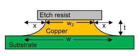
Chemical etching, no matter how tightly controlled, removes more material at the top of PCB trace walls, beneath the resist, than at the base.
A tightly controlled subtractive process results in traces that in cross-section are approximately a trapezoid with sides at a 25-45 degree included angle from the base and the base is at design width. However, if not closely regulated, bath chemistries can over-etch traces such that their top is much narrower than their base. The ratio between the height of the trace after etch (t) and how far the trace has been eaten away at the top of a wall (x) is the etch factor (F). The greater the etch factor, the closer a trace cross-section approaches rectangular. Bath chemistry can also vary from optimum such that not enough copper is removed, resulting in traces whose bases are wider than designed.
The closer a trace in cross-section along its full length conforms to a rectangle; the more predictable is its impedance. If traces could be repeatedly fabricated with nearly vertical sides at design width, the maximum circuit density could be achieved, signal integrity could be preserved, and board manufacturing yields could be optimum. An alternative to the subtractive process is the semi-additive fabrication process, which achieves those objectives and thereby enables a transition to much finer circuit geometries.
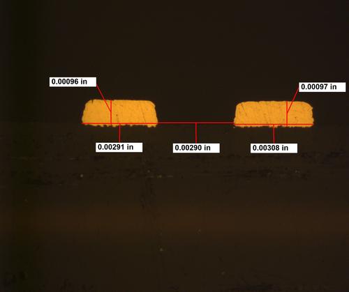
Each trace in this pair was designed to be 3 mils wide on 3-mil spacing. They were produced by a very well-controlled process and are the best that can be expected from subtractive fabrication.
Process details
Semi-additive PCB fabrication begins with as laminate that is clad with much thinner copper than the thinnest conventional foils: 2 or 3 microns thick, compared with quarter-ounce copper, which is approximately 8.5 microns thick. The ultra-thin copper sheets have a backing that is removed after the foil is laminated to a substrate. Via holes are drilled and then an electroless copper bath coats the bores and the copper surface. A resist is applied, developed, and selectively removed to expose only the areas that will become traces, vias, and other conductive features. Those exposed areas are plated up, the resist is removed, and the ultra-thin copper remaining in the spaces between the conductors is etched away. The process is essentially the opposite of subtractive PCB fabrication.Trace geometries are photolithography defined in the semi-additive process, in contrast to those resulting from subtractive fabrication, which are chemically defined. Consequently, trace widths and spaces created by the semi-additive process are virtually identical to as-designed dimensions. Trace width and spacing as fine as 1.25 mils can be maintained over distance within extremely tight tolerance, thereby maintaining strict impedance control. In fact, tests show impedance variation across an entire panel of boards does not exceed 0.5 ohm, one fifth that to be expected from well-controlled subtractive fabrication.
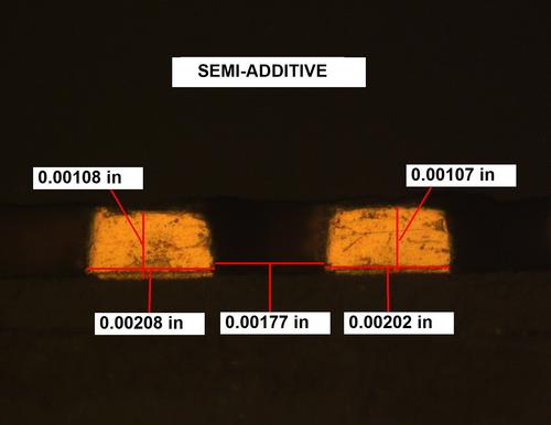
Note the near-vertical sides along a typical pair of 2-mil-wide traces on 1.8-mil spacing produced by the semi-additive process.
Precise impedance control is imperative to realize extremely high-speed digital systems and microwave applications and semi-additive fabrication affords that. Moreover, the near-vertical trace walls allow maximum circuit density.
Tags: PCB manufacturer, PCB supplier, PCB assembly, PCB design, Multilayer PCB, HDI PCB, LED PCB, Automotive PCB, High Frequency PCB. Industry Control PCB, PCBA, PCB Samples.