

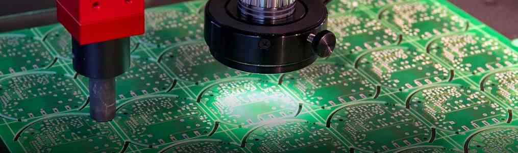
Through-hole technology (THT) is probably the oldest assembly technology in the field of PCB manufacturing. However, even in this modern age of surface-mounted technology (SMT), it still has its place. Even today, wired components are often assembled using wave soldering—in keeping with the tradition of times past. This has the disadvantage of requiring additional manufacturing equipment. It is therefore advisable to use reflow soldering for connectors and other wired components.
To this end, through-hole components were devised for automatic assembly and for high thermal loads in the furnace, which led to the birth of the term, through-hole reflow (THR). With this technology, it is now possible to process components in through-hole technology within the SMT process. But how can these solder joints be reliably tested? What technology is needed in order to be able to assess the solder penetration, for example?
Acceptance Criteria for THT/THR Solder Joints
Figure 1 is a schematic representation of a THT solder joint in cross-section. The solder wave flows from the solder source side to the solder target side (component side), due to capillary action. In so doing, it wets the connecting surface of the solder side, surrounds the pin and forms a solder meniscus on account of the protrusion of the pin on the solder side.
The acceptance criteria are defined in IPCA610 in order to distinguish between good and bad solder joints after successful soldering. Table 1 gives an overview of the criteria in excerpts.
It is now necessary to select testing technology which meets the specified acceptance criteria. Based on the example of a multi-row connector (Figure 2), the following table provides an overview of the test coverage of AOI and 3D AXI systems.
AOI systems are highly suited to assessment of the peripheral wetting of the pin and the sleeve and to evaluation of the wetted connecting surface on the solder side of a THT solder joint. The disadvantage of a traditional 2D AOI or an innovative 3D AOI system here, however, is that it is often only possible to assess the solder side because the pins on the component side are usually concealed by the component body itself. An assessment of the solder joints on the component side is therefore not possible with an AOI system. The solder penetration also remains hidden from traditional AOI technology.
A modern 3D X-ray system can provide a remedy. The 3D X-ray inspection not only makes the solder joints on the component side (i.e., below the component housing) visible, but is also able to calculate the solder penetration and the solder volume.
Tags: PCB manufacturer, PCB supplier, PCB assembly, PCB design, Multilayer PCB, HDI PCB, LED PCB, Automotive PCB, High Frequency PCB. Industry Control PCB, PCBA, PCB Samples.