

 Microfill through-hole fill (THF) electrolytic copper is a new process designed to offer outstanding through-hole fill, particularly for substrates intended for use as core layers in build¿Cup applications, producing planar, solid copper plugs in high-volume production plating equipment. This technology is intended to replace resin or paste plugging, and offers many advantages, including improved reliability, higher electrical and thermal conductivity, increased productivity and reduced process costs.
This paper describes a novel copper through-hole fill electroplating process designed for use with insoluble anodes and direct current (DC) rectification. The copper through-hole fill chemistry is formulated to operate over a broad range of operating conditions, and offers end-users outstanding production flexibility in either panel or pattern plate operating mode.
The paper addresses electrolytic copper through-hole filling performance for a variety of substrate thicknesses and hole diameters. The impact of the hole formation method and hole quality on filling ratio and void formation will be discussed. In this work, production scale tests were performed on 100 ª╠m and 200ª╠m thick substrates. The impacts of varying current density and solution flow on hole filling were examined. With optimized deposition conditions, including on-line additive analysis, void-free, highly planar through-hole filling and excellent bottom-up blind microvia filling with low surface copper deposition thickness were demonstrated.
Portability of consumer electronics has become the primary driver for the ever-increasing circuit density of todayí»s printed circuit designs. Based on the small dimensions of these devices, through-hole and blind via diameters are typically in the 75¿C150 ª╠m range. Performance improvement and process cost reduction make through-hole filling technology with copper an excellent approach, rather than the conventional plated through-hole.
Prior to the development of electrolytic copper through-hole filling, substrates for such applications were electroplated with a conventional through-hole process, then plugged with an epoxy material. Following these steps, additional planarization, re-metallization and electrolytic copper capping processes were required before the build-up process steps could begin.
Use of electrolytic copper through-hole filling eliminates several of these manufacturing steps and offers a number of additional advantages over the conventional build-up process by enhancing the thermal and electrical conductivity of the interconnections, and by reducing overall costs.
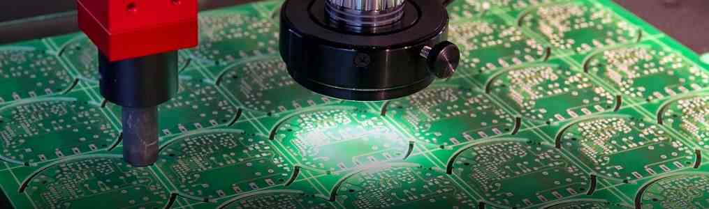
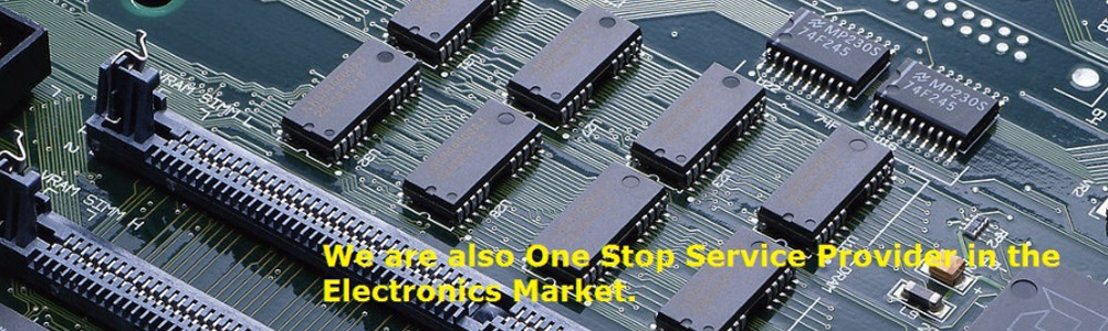
Tags: PCB manufacturer, PCB supplier, PCB assembly, PCB design, Multilayer PCB, HDI PCB, LED PCB, Automotive PCB, High Frequency PCB. Industry Control PCB, PCBA, PCB Samples.