

Figure 1, Solder side bottom of the LGA

Figure 2, CT image of the soldered LGA internal structure
Within the scope of the project, various X-ray methods (2D-X-Ray, laminography, X-ray CT) were used for comparative purposes in order to obtain evaluable data. In addition to the variations of the PCB design and the material parameters, the final vacuum pressure has been the overall influencing factor on the minimization of the void content (Fig. 3). With decreasing pressure in the environment of the molten solder joints, their void content decreases significantly.
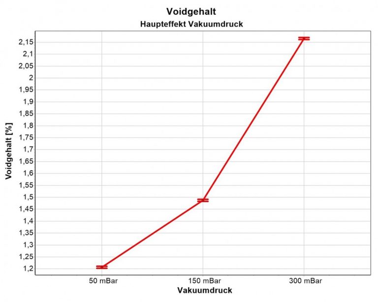
Figure 3, Influence of the final vacuum pressure on the pore content
In general, good LGA solder joints could be produced. The solder wetting of both the LGA connections and the PCB pads was uncritical, as the metallographic investigations prove. The solder gap characteristics essentially correspond to theoretical expectations and the variance is more influenced by the design of the PCB pads than by the voids. The microsections produced reveal the details of the topography of both joining partners, the printed circuit board and the LGA.
Figure 4 shows a section of an LGA32 solder joint in darkfield contrast on which the dimensions of the respective solder resist masks and the gap remaining between them are dimensioned. Only these remaining 13 μm allow the LGA to float in (self-centering) during soldering. Tolerances in the general manufacturing process can further shrink this gap so that both solder resist masks lie on top of each other, making it impossible for the LGA to self-centering.

Figure 4, Dark field image of an LGA solder joint
(Photos: Rehm Thermal Systems).